본문바로가기
닫기
Company Profile
CEO's Message
Vision
History
Technology Research Center
Organization
Partner Firms and Customers
Location
Business Area
Semiconductor
Display
Eco-friendly energy
General
Product
Semiconductor
Display
Eco-friendly energy
General
IR
Notices
Disclosure
Customer Service Center
Notice
Archive
Inquiries
LANGUAGE
KO
EN
CN
Semiconductor
Display
Eco-friendly energy
General
Semiconductor
All
I-Line Photoresist
Bump Photoresist
KrF Photoresist
TSV Thick Photoresist
BARC
TARC
Developer
Etchant
Promoter
Rinsing Solution
Spin On Carbon Hardmask
CMP
Wafering
A Total of
10
hit(s)
Subject
Contents
Name
I-Line Photoresist
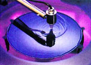
We manufacture i-line photoresist products for process applications with film thickness from 0.1um to 6.0um in relation to 365nm wavelength. We manufacture positive and negative type i-line photoresist solutions in the i-line photoresist product line-up. If you are looking for an i-line photoresist solution for project development, we will provide more specific data on the product line-up when you make an inquiry to us.
YCIP-4000E
-Target : Thickness 3.5um (Res. 1.5um & 3.0um, 1:1)
-Purpose of use : Implant & Metal Layer
YCIP-1700
-Target : Thickness 1.7um (Res. 500nm, 1:1)
-Purpose of use : Implant & Etch Layer / OLED Devices
YCIP-1300
-Target : Thickness 1.3um (Res. 500nm, 1:1)
-Purpose of use : Implant & Etch Layer / OLED Devices
YCIP-1100
-Target : Thickness 1.1um (Res. 500nm, 1:1)
-Purpose of use : Implant & Etch Layer / OLED Devices
YCIN-2000/YCIN-6000
-Target : Thickness 2.0um ~ 6.0um (Bulk Pattern)
-Purpose of use : Implant & Etch Layer / OLED Devices
YCIN-1000
-Target : Thickness 1.0um (Res. 500nm, 1:1)
-Purpose of use : Implant & Etch Layer / OLED Devices
YCIN-600
-Target : Thickness 6.0um (Res. 500nm, 1:1)
-Purpose of use : Implant Layer
YCIN-350
-Target : Thickness 0.17um (Res. 500um, 1:1)
-Purpose of use : Passivation Photoresist
YCIN-130
-Target : Thickness 0.1um (Res. 1.0um, 1:1)
-Purpose of use : Passivation Photoresist
1