본문바로가기
닫기
Company Profile
CEO's Message
Vision
History
Technology Research Center
Organization
Partner Firms and Customers
Location
Business Area
Semiconductor
Display
Eco-friendly energy
General
Product
Semiconductor
Display
Eco-friendly energy
General
IR
Notices
Disclosure
Customer Service Center
Notice
Archive
Inquiries
LANGUAGE
KO
EN
CN
Semiconductor
Display
Eco-friendly energy
General
Semiconductor
All
I-Line Photoresist
Bump Photoresist
KrF Photoresist
TSV Thick Photoresist
BARC
TARC
Developer
Etchant
Promoter
Rinsing Solution
Spin On Carbon Hardmask
CMP
Wafering
A Total of
62
hit(s)
Subject
Contents
Name
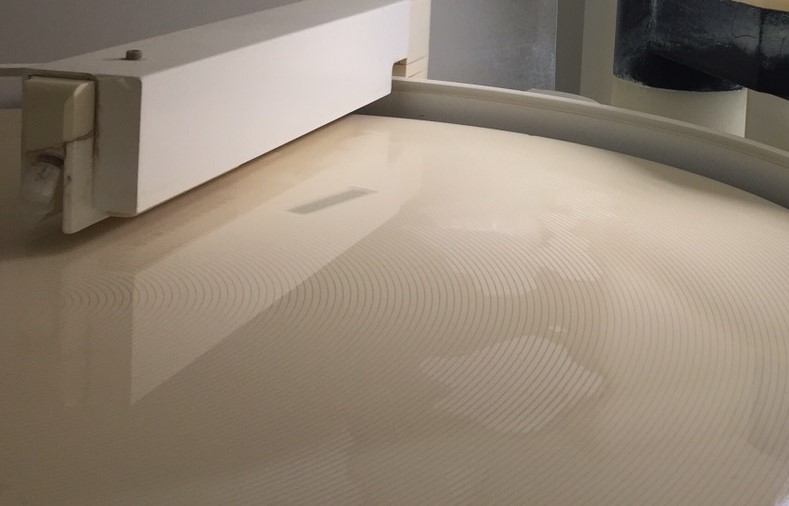
Wafering
Wafering is a process of making silicon crystal into wafer. The process is generally performed by a multi-wire saw, which cuts multiple wafers concurrently of the same crystal. Eventually, the wafer is polished to the desired evenness and thickness
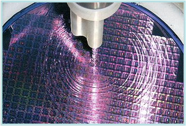
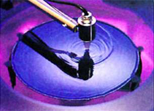
CMP
CMP (Chemical Mechanical Planarization or Polishing) is used in all semiconductor processes: making the insulation films different even due to element wiring or separating the element wiring by distributing the slurry containing hundreds of nm size polishing abrasives on the polishing pad surface. This induces the film's chemical reactions, and mechanically removing the transformed film surface by rotating the wafer-supporting polishing carrier and the polishing plate with the polishing pad attached at a high speed, when the wafer is stuck to the polishing pad with poly-urethane.
Spin On Carbon Hardmask
As the pattern size of a semiconductor element is reduced, if the thickness is reduced using the existing PR in implementing a pattern of less than 70nm, when the pattern is engraved at the depth required in the etch process, there is a possibility of the photoresist collapsing. To improve this, an SOC polymer is used. Although the pattern is engraved on the SOC polymer layer at the depth required for the each process using the photoresist, this can be used as a support material to prevent a photoresist collapse.
Rinsing Solution
As a material used in the photo process, this is a material used to prevent pattern damage that occurs while rinsing with D.I. water, after the developer process.
Etchant
This is a material used to remove unnecessary metals existing on the PCB through chemical reactions.
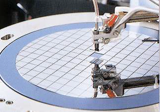
Developer
As a material used in the last stage of the photo development process, this product is a material used in the process of forming patterns on the circuit by selectively removing the exposed areas and non-exposed areas.
TARC
The even pattern can only be formed if the reflectivity is maintained at less than 1%, while the exposure process is being carried out by the reduction of the pattern size of the semiconductor element (Top Anti Reflective Coating). This is used to improve the reflective light and diffused reflection occurrence within the photoresist film during the pattern forming using lithography by treating the prevention film of reflection on the top part upon exposure.
BARC
The even pattern can only be formed if the reflectivity is maintained at less than 1% while the exposure process is being carried out by the reduction of the pattern size of the semiconductor element (Top Anti Reflective Coating). During the pattern forming using lithography, the product is a light absorption agent used for the prevention of reflection and refined wave removal through the lower part of the film layer, and is an organic reflection prevention film.
TSV Thick Photoresist
We have developed and commercialized photoresists for various packaging processes including the latest technology. The photoresists for packaging processes can be used for extensive production technologies such as wafer level RDL and TSV.
KrF Photoresist
We manufacture KrF photoresists for process application with 0.30um to 12.0um of film thickness in relation to 248nm wavelength. In the KrF photoresist product line, we manufacture both positive and negative type photoresists. If you are looking for a krF photoresist solution for project development, we will provide more specific data for the product line when you make an inquiry to us.
Bump Photoresist
We supply positive and negative tone photoresists designed to meet the narrow pitch of related products, such as the recently developed wafer level packaging, MEMs, and 3D photolithography. The photoresist is compatible with various metals' plated chemicals including copper, pure tin, and nickel.
I-Line Photoresist
We manufacture i-line photoresist products for process applications with film thickness from 0.1um to 6.0um in relation to 365nm wavelength. We manufacture positive and negative type i-line photoresist solutions in the i-line photoresist product line-up. If you are looking for an i-line photoresist solution for project development, we will provide more specific data on the product line-up when you make an inquiry to us.
AYCKP-9160
-Target : Thickness 6.0um (Res. 5.0um, Contact Hole)
-Purpose of use : KrF Positive TSV Devices
YSO-800
YSO-800 is an oil-based cutting fluid used in wafer cutting, ensuring excellent cooling, lubricity, extreme pressure, and rust resistance functions. It also has excellent effect on maintaining appropriate viscosity and compressive sedimentation prevention of SiC slurry.
YPCC-2000
Cleaning the wafer surface contamination and anti-corrosion control after the CMP process.
1
2
3
4
5