본문바로가기
닫기
Company Profile
CEO's Message
Vision
History
Technology Research Center
Organization
Partner Firms and Customers
Location
Business Area
Semiconductor
Display
Eco-friendly energy
General
Product
Semiconductor
Display
Eco-friendly energy
General
IR
Notices
Disclosure
Customer Service Center
Notice
Archive
Inquiries
LANGUAGE
KO
EN
CN
Semiconductor
Display
Eco-friendly energy
General
Semiconductor
All
I-Line Photoresist
Bump Photoresist
KrF Photoresist
TSV Thick Photoresist
BARC
TARC
Developer
Etchant
Promoter
Rinsing Solution
Spin On Carbon Hardmask
CMP
Wafering
A Total of
8
hit(s)
Subject
Contents
Name
CMP
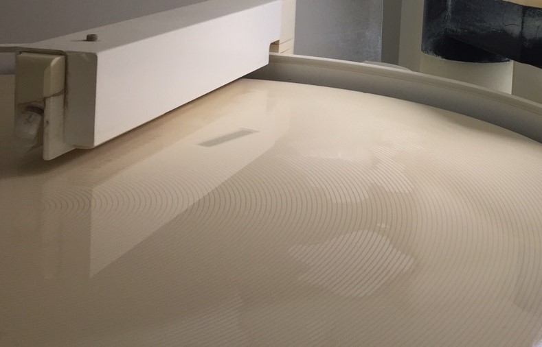
CMP (Chemical Mechanical Planarization or Polishing) is used in all semiconductor processes: making the insulation films different even due to element wiring or separating the element wiring by distributing the slurry containing hundreds of nm size polishing abrasives on the polishing pad surface. This induces the film's chemical reactions, and mechanically removing the transformed film surface by rotating the wafer-supporting polishing carrier and the polishing plate with the polishing pad attached at a high speed, when the wafer is stuck to the polishing pad with poly-urethane.
YPCC-2000
Cleaning the wafer surface contamination and anti-corrosion control after the CMP process.
YCBW-H609
Low selectivity of tungsten layer polishing for the purpose of effective tungsten surface buffing and scratch remove.
YCLW-S804
Tunable selective polishing slurry for the tungsten/oxide layer and minimum dishing.
YCHT-S902
High selective polishing slurry for bulk tungsten remove and minimum erosion.
SD-100
Polishing slurry for the Cu barrier metals layer remove accompanied by corrosion and scratch control.
YCHC-S711
High selective polishing slurry for bulk Cu remove accompanied by corrosion control.
NTS-300
-Polishing slurry for the multiple layer of SiO2/Poly/Nitride.
-Alternative of selective/non-selective polishing.
1